- 您现在的位置:买卖IC网 > Sheet目录2006 > LTC2606IDD#TRPBF (Linear Technology)IC DAC 16BIT I2C V-OUT 10-DFN
LTC2606/LTC2616/LTC2626
3
26061626fb
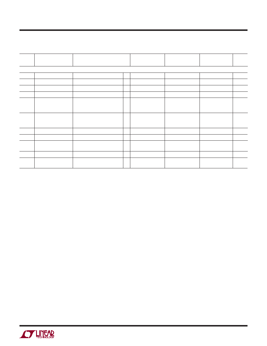
ELECTRICAL CHARACTERISTICS The ● denotes specications which apply over the full operating
temperature range, otherwise specications are at TA = 25°C. REF = 4.096V (VCC = 5V), REF = 2.048V (VCC = 2.7V), VOUT unloaded,
unless otherwise noted.
LTC2626/LTC2626-1
LTC2616/LTC2616-1
LTC2606/LTC2606-1
SYMBOL PARAMETER
CONDITIONS
MIN
TYP
MAX
MIN
TYP
MAX
MIN
TYP
MAX
UNITS
DC Performance
Resolution
●
12
14
16
Bits
Monotonicity
(Note 2)
●
12
14
16
Bits
DNL
Differential Nonlinearity
(Note 2)
●
±0.5
± 1
±1
LSB
INL
Integral Nonlinearity
(Note 2)
●
± 1
±4
±16
±14
±64
LSB
Load Regulation
VREF = VCC = 5V, Mid-Scale
IOUT = 0mA to 15mA Sourcing
IOUT = 0mA to 15mA Sinking
●
0.025
0.05
0.125
0.1
0.2
0.5
0.7
2
LSB/mA
VREF = VCC = 2.7V, Mid-Scale
IOUT = 0mA to 7.5mA Sourcing
IOUT = 0mA to 7.5mA Sinking
●
0.05
0.1
0.25
0.2
0.4
1
0.9
1.5
4
LSB/mA
ZSE
Zero-Scale Error
Code = 0
●
19
1
9
1
9
mV
VOS
Offset Error
(Note 5)
●
±1
±9
±1
±9
±1
±9
mV
VOS Temperature
Coefcient
±5
μV/°C
GE
Gain Error
●
±0.1
±0.7
±0.1
±0.7
±0.1
±0.7
%FSR
Gain Temperature
Coefcient
±8.5
ppm/°C
发布紧急采购,3分钟左右您将得到回复。
相关PDF资料
LTC2607IDE#TRPBF
IC DAC 16BIT R-R I2C 12-DFN
LTC2609CGN#PBF
IC DAC 16BIT R-R QUAD 16SSOP
LTC2621IDD-1#PBF
IC DAC 12BIT R-R 10-DFN
LTC2630HSC6-LZ12#TRPBF
IC DAC 12BIT R-R SC70-6
LTC2642IDD-16#PBF
IC DAC 16BIT VOUT 10-DFN
LTC2704IGW-16#PBF
IC DAC 16BIT QUAD VOUT 44-SSOP
LTC2751AIUHF-16#PBF
IC DAC 16BIT CUR OUT 38-QFN
LTC2752ACLX#PBF
IC DAC 16BIT DUAL CUR OUT 48LQFP
相关代理商/技术参数
LTC2606IDD-1
制造商:Linear Technology 功能描述:DAC 1-CH 16-bit 10-Pin DFN EP
LTC2606IDD-1#PBF
功能描述:IC DAC 16BIT I2C V-OUT 10-DFN RoHS:是 类别:集成电路 (IC) >> 数据采集 - 数模转换器 系列:- 产品培训模块:LTC263x 12-, 10-, and 8-Bit VOUT DAC Family 特色产品:LTC2636 - Octal 12-/10-/8-Bit SPI VOUT DACs with 10ppm/°C Reference 标准包装:91 系列:- 设置时间:4µs 位数:10 数据接口:MICROWIRE?,串行,SPI? 转换器数目:8 电压电源:单电源 功率耗散(最大):2.7mW 工作温度:-40°C ~ 85°C 安装类型:表面贴装 封装/外壳:14-WFDFN 裸露焊盘 供应商设备封装:14-DFN-EP(4x3) 包装:管件 输出数目和类型:8 电压,单极 采样率(每秒):*
LTC2606IDD-1#TRPBF
功能描述:IC DAC 16BIT I2C V-OUT 10-DFN RoHS:是 类别:集成电路 (IC) >> 数据采集 - 数模转换器 系列:- 产品培训模块:LTC263x 12-, 10-, and 8-Bit VOUT DAC Family 特色产品:LTC2636 - Octal 12-/10-/8-Bit SPI VOUT DACs with 10ppm/°C Reference 标准包装:91 系列:- 设置时间:4µs 位数:10 数据接口:MICROWIRE?,串行,SPI? 转换器数目:8 电压电源:单电源 功率耗散(最大):2.7mW 工作温度:-40°C ~ 85°C 安装类型:表面贴装 封装/外壳:14-WFDFN 裸露焊盘 供应商设备封装:14-DFN-EP(4x3) 包装:管件 输出数目和类型:8 电压,单极 采样率(每秒):*
LTC2607CDE#PBF
功能描述:IC DAC 16BIT R-R I2C 12-DFN RoHS:是 类别:集成电路 (IC) >> 数据采集 - 数模转换器 系列:- 产品培训模块:Lead (SnPb) Finish for COTS
Obsolescence Mitigation Program 标准包装:50 系列:- 设置时间:4µs 位数:12 数据接口:串行 转换器数目:2 电压电源:单电源 功率耗散(最大):- 工作温度:-40°C ~ 85°C 安装类型:表面贴装 封装/外壳:8-TSSOP,8-MSOP(0.118",3.00mm 宽) 供应商设备封装:8-uMAX 包装:管件 输出数目和类型:2 电压,单极 采样率(每秒):* 产品目录页面:1398 (CN2011-ZH PDF)
LTC2607CDE#TRPBF
功能描述:IC DAC 16BIT R-R I2C 12-DFN RoHS:是 类别:集成电路 (IC) >> 数据采集 - 数模转换器 系列:- 标准包装:47 系列:- 设置时间:2µs 位数:14 数据接口:并联 转换器数目:1 电压电源:单电源 功率耗散(最大):55µW 工作温度:-40°C ~ 85°C 安装类型:表面贴装 封装/外壳:28-SSOP(0.209",5.30mm 宽) 供应商设备封装:28-SSOP 包装:管件 输出数目和类型:1 电流,单极;1 电流,双极 采样率(每秒):*
LTC2607CDE-1#PBF
功能描述:IC DAC 16BIT R-R I2C 12-DFN RoHS:是 类别:集成电路 (IC) >> 数据采集 - 数模转换器 系列:- 标准包装:47 系列:- 设置时间:2µs 位数:14 数据接口:并联 转换器数目:1 电压电源:单电源 功率耗散(最大):55µW 工作温度:-40°C ~ 85°C 安装类型:表面贴装 封装/外壳:28-SSOP(0.209",5.30mm 宽) 供应商设备封装:28-SSOP 包装:管件 输出数目和类型:1 电流,单极;1 电流,双极 采样率(每秒):*
LTC2607CDE-1#TRPBF
功能描述:IC DAC 16BIT R-R I2C 12-DFN RoHS:是 类别:集成电路 (IC) >> 数据采集 - 数模转换器 系列:- 标准包装:2,400 系列:- 设置时间:- 位数:18 数据接口:串行 转换器数目:3 电压电源:模拟和数字 功率耗散(最大):- 工作温度:-40°C ~ 85°C 安装类型:表面贴装 封装/外壳:36-TFBGA 供应商设备封装:36-TFBGA 包装:带卷 (TR) 输出数目和类型:* 采样率(每秒):*
LTC2607IDE#PBF
功能描述:IC DAC 16BIT R-R I2C 12-DFN RoHS:是 类别:集成电路 (IC) >> 数据采集 - 数模转换器 系列:- 标准包装:1 系列:- 设置时间:4.5µs 位数:12 数据接口:串行,SPI? 转换器数目:1 电压电源:单电源 功率耗散(最大):- 工作温度:-40°C ~ 125°C 安装类型:表面贴装 封装/外壳:8-SOIC(0.154",3.90mm 宽) 供应商设备封装:8-SOICN 包装:剪切带 (CT) 输出数目和类型:1 电压,单极;1 电压,双极 采样率(每秒):* 其它名称:MCP4921T-E/SNCTMCP4921T-E/SNRCTMCP4921T-E/SNRCT-ND